Welcome to visit our website, Safe De Technology !


》》Application range
Mobile phone, communication, POS Tablet, car, medical, aviation Office equipment, industrial control, etc.
》》Technical Skills
Minimum PCB thickness (12-layer HDI): 0.7mm; Minimum hole ring: 0.06mm; Welding tolerance: +-0.02; Base copper 1/4 oz: 0.03/0.03mm

Wechat Scan
Tel:86-755-23290283
Fax:86-755-23290282
E-mail:tomgao@safe-de.com
Trusted by hundreds of companies
Custom PCB consistently choose us


Tel:86-755-23290283
E-mail:tomgao@safe-de.com
Address:Room 302, Block A , Jiepeng Business Plaza, Fenghuang community, Fuyong 518103 Shenzhen, Guangdong China
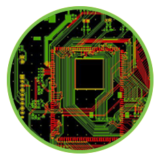
IC carrier PCB high-precision multi-layer multi-level HDI any interconnected HDI high-precision multi-layer multi-level module half-hole HDI high-precision multi-layer through-hole PCB


 8layer")
 6 Layer structure")
")